Rehan Kapadia
Director MOSIS 2.0
| Foundry Service | Technology Node | Tapeout Date |
|---|---|---|
| TSMC | 22 nm | 3/4/2026 |
Rapid prototyping and process development capability through access to seven university nanofabrication facilities and other experimental prototyping facilities within the Southern California area and throughout the nation.
Supporting both silicon CMOS and advanced compound semiconductor technologies with seamless access to a wide array of commercial silicon MPW services from leading large, medium, and small-volume foundries.
Providing comprehensive chip design services that simplify and streamline the development process, enabling customers to bring their innovative ideas from concept to silicon.
More event details coming soon.
Don’t miss out on this opportunity to engage with MOSIS 2.0 to accelerate your semiconductor circuit design and prototyping projects.
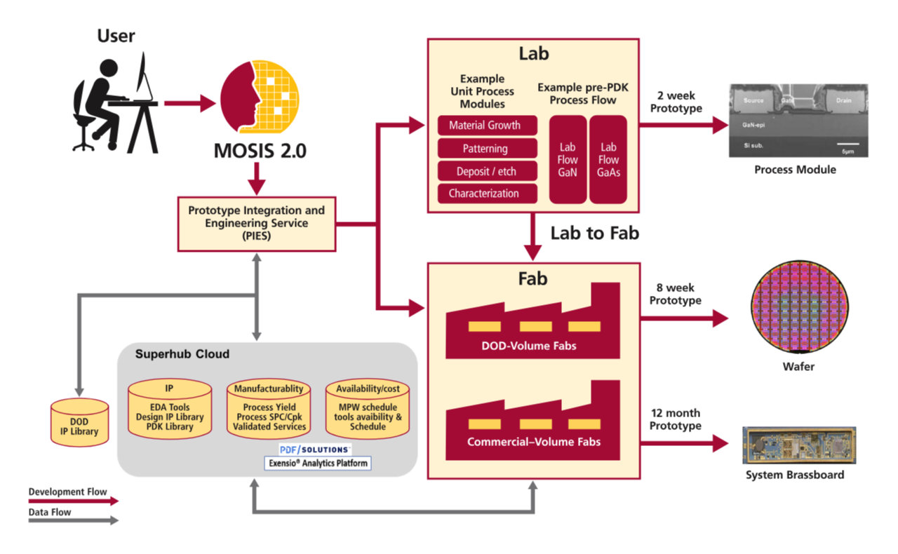
Fill Out Our Interest FormMOSIS 2.0 is the central storefront and gateway to access cutting-edge prototyping services, targeting advanced RF, 5G/6G, and EW applications.
The Prototype Integration and Engineering Service (PIES) Team is at the core of MOSIS 2.0 - a dedicated fab-knowledgeable engineering group that supports designers to accelerate their innovations to solutions.
We invite innovators, researchers, and industry partners to engage with MOSIS 2.0-and join us in advancing next-generation microelectronics.
Director MOSIS 2.0
Fabrication Services
Team Lead
Senior Project Manager
MPW Services Team Lead
Receive notifications for new MOSIS 2.0 offerings and upcoming MPW runs.
Are you passionate about advancing semiconductor design infrastructure? We have an exciting opening on the MOSIS 2.0 PIES Team at USC/ISI.
📍 Los Angeles, CA (On-site at USC University Park Campus)
💼 Full-Time | Salary: $156,918 – $180,000
What You'll Do:
🔹 Maintain and optimize multi-vendor EDA tool flows for digital design
🔹 Manage cloud platforms for EDA tools and IP repositories
🔹 Support users across the MOSIS 2.0 hub and partner ecosystem
You're a Great Fit If You Have:
✔ Experience with EDA tools from vendors like Ansys, Cadence, Siemens, Synopsys
✔ Cloud platform experience for EDA deployment
✔ Master's degree in EE or related field
✔ U.S. citizenship or permanent residency (ITAR/EAR required)
Apply now: https://lnkd.in/gVCEBSs7
Know someone perfect for this? Share away!
Our booth is #11 and we will be open Tuesday 8-5 PST and Wednesday 8-11 PST.
We hope to see you there!
Two years into California DREAMS, USC Information Sciences Institute's Computational Systems Division is tackling one of the biggest challenges in chip development: the "valley of death" between brilliant ideas and working prototypes.
The problem? Modern semiconductor designs require expensive IP licenses, complex toolchains, and expertise in peripheral technologies that pull innovators away from their breakthrough ideas. A single chip can demand hundreds of thousands of dollars in licensing costs alone.
Our solution combines three strategic approaches:
Rapid Design Generation → Platform SoC generators that can produce complete architectures in hours instead of months, enabling parallel design space exploration
Comprehensive IP Repository → Silicon-verified processors, accelerators, and specialized cores including our DARPA-developed high-speed DSP and homomorphic encryption IP
Accelerated Prototyping → FPGA-based platforms (MAPP) that dramatically reduce pre- and post-fabrication testing complexity and cost
What sets us apart: we're a DMEA-accredited trusted IC supplier with CMMC accreditation, combining university research agility with the security credentials and infrastructure to support sensitive government projects.
The result? Research teams can focus on their core innovations while we handle the increasingly complex infrastructure demands. We're restoring semiconductor development to its innovation-focused roots.
Read the full story about how MOSIS 2.0 is transforming the semiconductor development ecosystem → https://lnkd.in/gKmDm8D4
Check out our video recap https://lnkd.in/grQvmwVf
Our expert panel brought together leaders shaping the future of U.S. microelectronics:
✨ Tim Morgan – Technical Director, Microelectronics Commons
✨ Eric Makara – 5G/6G Lead, Microelectronics Commons
✨ Scott Bukofsky – Senior VP, Microelectronics, NSTXL (National Security Technology Accelerator)
✨ Victor Mai – Deputy Director, Microelectronics Commons at NSTXL (National Security Technology Accelerator)
In a recent talk, Rehan Kapadia, director of MOSIS 2.0, laid out a bold roadmap for the future of rapid microelectronics prototyping, one that reinvigorates the original MOSIS spirit while meeting the complexity of today’s semiconductor landscape.
Kapadia traced the origins of MOSIS back to 1981, when it democratized chip fabrication by giving researchers access to multi-project wafers. Today, he explained, the challenges are bigger, and so are the opportunities.
Here are the key takeaways from his talk:
✨ A national ecosystem, not just a service
MOSIS 2.0 is connecting universities, fabs, advanced packaging houses, photonics facilities, and industry partners to streamline the full journey from concept to hardware.
🔧 Lowering barriers to prototyping — again
Just as the original MOSIS opened the door for CMOS design, MOSIS 2.0 is expanding that access to heterogeneous integration, advanced packaging, photonics, and more.
🤝 Hands-on support through the PIES team
Kapadia emphasized that designers don’t need to arrive with a finished GDS — MOSIS 2.0 guides teams from early idea to manufactured prototype.
📈 Data-driven fabrication
By leveraging shared data and coordinated processes, the network aims to reduce risk, shorten cycles, and make prototyping more predictable across facilities.
Kapadia closed with a clear message: Innovation accelerates when access expands. And MOSIS 2.0 is here to make that access real.
👉 Learn more about his talk and the vision behind MOSIS 2.0 here: https://lnkd.in/gApe2Nuh