

Advanced Foundry Capabilities Through MOSIS 2.0
USC-led semiconductor prototyping initiative MOSIS 2.0 will be the official storefront for cutting-edge foundry services from domestic microelectronics leaders.
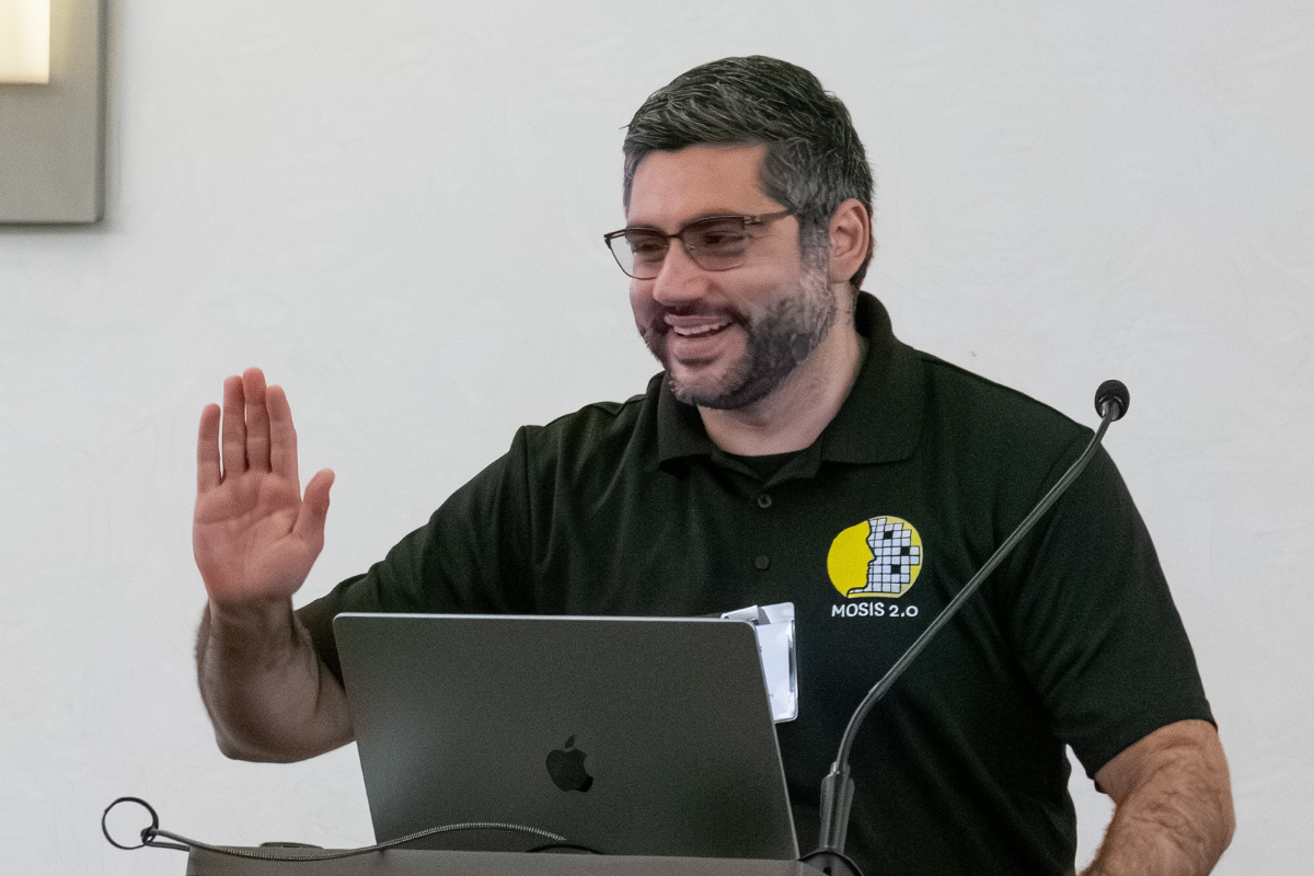
MOSIS 2.0 Director Rehan Kapadia joined the latest episode of the Micro Journeys Podcast, where he discussed the intersection of imagination, engineering, and access in the world of microelectronics.
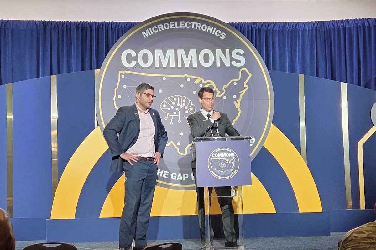
The USC-led semiconductor superhub highlighted its innovation and workforce development leadership at the 2026 Microelectronics Commons Annual Meeting in Washington, D.C.
Rehan Kapadia, director of MOSIS 2.0, shared how the service is building on its pioneering legacy to create a national network that lowers barriers, accelerates prototyping, and drives U.S. innovation in microelectronics.
As CA DREAMS’ semiconductor fabrication service transitions to full-scale operations, Rehan Kapadia, a longtime faculty contributor and director of the USC John O’Brien Nanofabrication Laboratory, is named the new Director of MOSIS 2.0. Kapadia brings a strong vision for advancing MOSIS 2.0’s mission to accelerate semiconductor prototyping.
In 2025, MOSIS 2.0, is significantly expanding its semiconductor prototyping capabilities beyond Southern California to include technologies from two additional technology hubs: the Southwest Advanced Prototyping (SWAP) Hub, led by the Arizona Board of Regents on behalf of Arizona State University, and the Midwest Microelectronics Consortium (MMEC) Hub in Ohio.
UC San Diego’s work is part of the California DREAMS hub, a Southern California regional coalition of universities, contractors and workforce-development organizations led by the USC Viterbi School of Engineering and its Information Sciences Institute (ISI).
Over four decades, MOSIS delivered more than 60,000 integrated circuit designs and generated up to $10 million annually at its peak. Now, its successor, MOSIS 2.0, is advancing this legacy to address the next-generation of chip innovation.
The Department of Defense has awarded an additional $27 million from the CHIPS & Science Act to CA DREAMS. This continued investment will further support CA DREAMS in advancing U.S. semiconductor capabilities by expanding its infrastructure, operations, and workforce development.
Troubleshooting for secondary source materials can often be time and labor intensive, taking up to a year to solve. In a Pipe Cleaner project, Hub partners University of California, San Diego and Northrop Grumman worked together to find a substitute process material. The promising result took months off their normal timeline.
Receive notifications for new MOSIS 2.0 offerings and upcoming MPW runs.